


MF RC500 card reader chip circuit
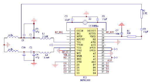
EMC low-pass filtering: L1, L2, C3, C4 form the EMC low-pass filtering circuit. Due to the RF card reader chip operating at 13.56MHz, it generates a clock signal from a crystal oscillator at 13.56MHz, and the signal sent to the antenna is also an energy carrier signal at 13.56MHz. Therefore, in addition to the 13.56MHz signal, the emitted signal also emits some high-order harmonics, and some international EMC standards do not allow circuit boards to emit interference signals externally. Therefore, it is necessary to design a suitable low-pass filter to meet EMC requirements. It is recommended to use a multi-layer board to design the antenna section, as this will also improve its EMC performance.
Antenna impedance matching: C1, C2, C9, and C10 are used to match antenna impedance. Due to the impedance conversion of the low-pass filtering circuit, the antenna section should also be tuned to match this impedance. Adjust the values of these capacitors to achieve the best impedance matching of the designed antenna (usually set at 50 ohms).
Receiving circuit: The chip demodulates the subcarrier transmitted by the card internally. No external filtering circuit is required. R1 is used to provide a DC bias level at the input of RX (the input pin of the operational amplifier). C7 is used for decoupling. The voltage division of R2+C8 and R1 forms the AC signal input, and their values are influenced by the antenna design and impedance matching. Therefore, it is recommended to use the manufacturer's recommended values. If necessary, R2 can be adjusted to change the AC input level at the RX end.
Antenna: The left colla and collb are actually several turns of coils on the printed circuit board, used as antennas for card readers.
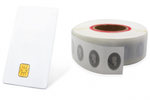
Related PProducts


Page
Hot News

