Label packaging technology
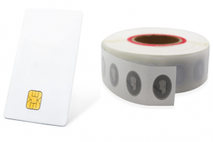
In China, the packaging of labels mostly adopts full package technology, which means that IC chips and etched antennas are protected by thin films such as polystyrene. This process has the characteristics of low cost, high packaging efficiency, flexible and convenient construction, simple process control, and high automation program. Not only can it solve the urgent problems of variable processing batches, high density, and low-cost packaging in the microelectronics industry, but it also provides stable quality and reliable performance for the currently booming flexible production of electronic labels. The only drawback is that compared to similar foreign products, its thickness has slightly increased. However, this does not affect the electrical characteristics and performance of electronic tags. In addition, in the interconnection process between antennas and chips, due to the small and ultra-thin chips, a more appropriate method is to use flip chip technology on the antenna interface, which has the characteristics of high production efficiency, miniaturization, and high reliability of connection. To adapt to flexible substrate materials, the inverted bonding material needs to use special conductive adhesive to achieve ACA interconnection between chips and antenna pads. However, the price of ACA materials in the market is currently relatively expensive, with a price of over 2000 RMB for 5 milligrams of ACA material. However, the ACA interconnect process may reduce processes and shorten production time. If a new type of conductive adhesive with low cost can be produced to meet the interconnection of electronic tag circuits, ACA interconnection may also become a low-cost choice.


